




![Busy port scene with stacked shipping containers, large cranes, and cargo ships in a bay, beside a coastal highway and rail line on the right.] }} (Note: The input requires a valid JSON with an array of strings in altTexts. Here is a corrected version.)Let's provide proper JSON.](https://www.supplychaininforms.com/wp-content/uploads/2026/09/trade-and-logistics-infrastructure-218x150.webp "Turkey Looks to Upgrade Trade and Logistics Infrastructure")























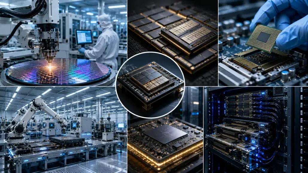
Samsung Electronics Co. has entered into a $200 billion strategic partnership with Broadcom Inc., the U.S. chip designer so as to create a fully integrated chip supply chain for artificial intelligence – AI semiconductors through 2030.
On July 24, 2026, both the companies executed an MOU so as to build next-generation AI infrastructure at the San Francisco AI Summit, which was hosted by the Korean government in San Francisco.
As part of the agreement, Samsung is going to provide Broadcom an integrated one-stop supply solution that integrates its HBM4 and HBM4E memory and sub-2-nanometer foundry processes as well as advanced packaging technologies for the next-generation AI accelerators as well as high-speed networking chips.
The companies intend to deepen their partnership in the areas of memory, foundry, and packaging in a period of five years.
The partnership is representative of a wider trend in the AI semiconductor market away from the graphics processing unit – GPU-based systems of Nvidia Corp. towards bespoke AI accelerators or application-specific integrated circuits – ASICs being created by big technology companies. The AI semiconductor revenue of Broadcom was $10.8 billion in the 2nd quarter of fiscal 2026, upward 143% YOY.
Broadcom is projected to generate $16 billion in AI chip sales in the third quarter, and customer demand for custom accelerators and AI networking chips is likely to continue to rise.
There is a growing need for manufacturing partners that integrate memory and compute chips as well as advanced packaging into one solution, industry analysts said.
The partnership will likely benefit Samsung in a variety of ways. A broader clientele for HBM might reduce its dependence on a single customer, whereas successful mass production of sub-2-nanometer chips for a key client could demonstrate the manufacturing yields and process reliability of the company, which could help it secure more foundry orders, analysts said.
Also seen as a boost to customer connections beyond sales of individual products is expected to be the combination of memory, foundry manufacturing, and advanced packaging in one offering, and greater collaboration might shorten development cycles while decreasing power consumption.
The partnership has also raised hopes that Samsung might emerge as a replacement to the advanced foundry and packaging ecosystem currently controlled by Taiwan Semiconductor Manufacturing Co. With HBM integration as well as advanced packaging becoming more crucial for performance in general in the AI accelerator market, the entry from Samsung could help minimise manufacturing bottlenecks, decrease supply chain density, and enhance price and delivery rivalry.
An industry official remarked that the partnership to fully integrated chip supply chain sets the stage for Samsung to emerge as an integrated AI semiconductor supplier across memory and foundry, but its performance will rely on customer qualification, advanced packaging capacity, 2-nanometer yields, and of course, final order volumes.